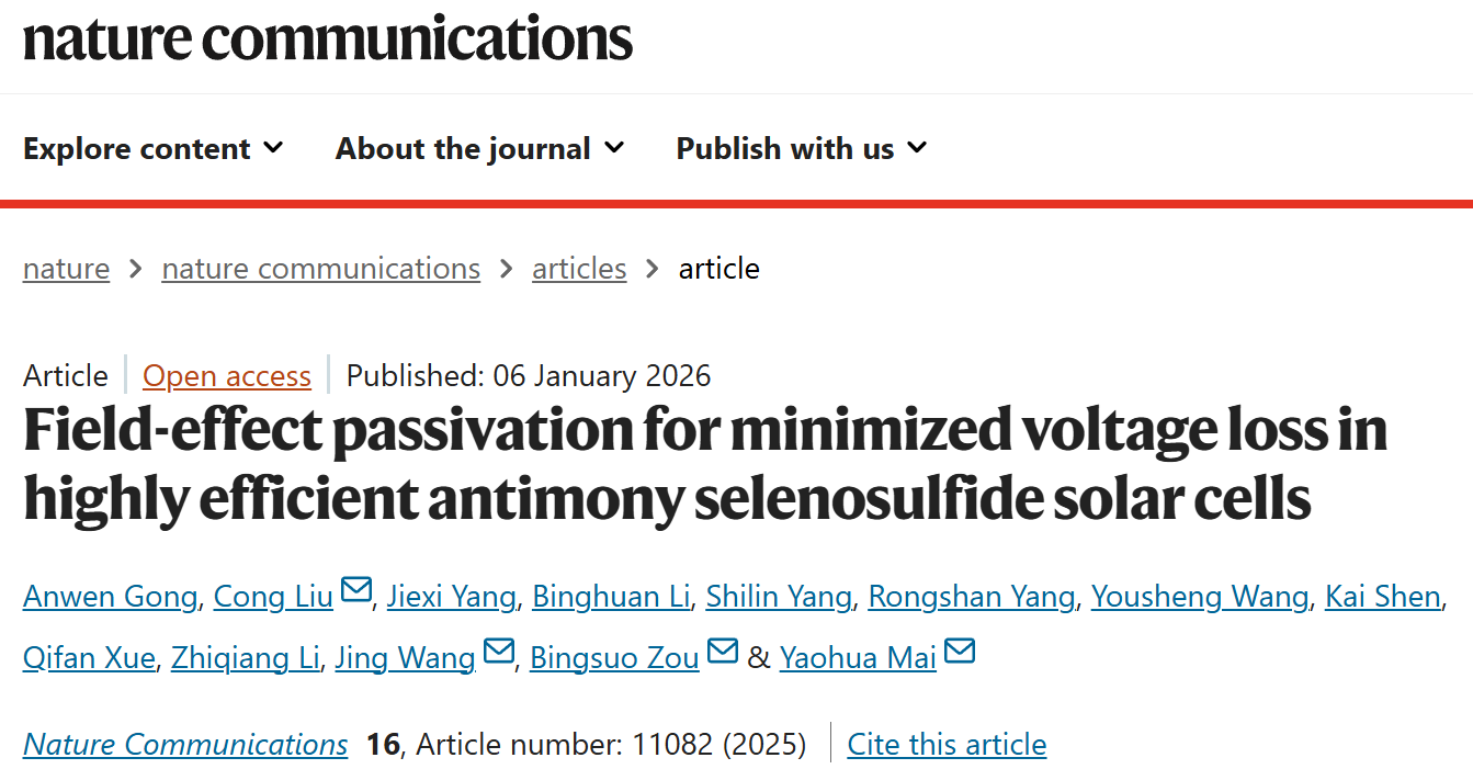
Recently, the Nano Photonics Materials and Technology Team at GXU has made new progress in the field of antimony selenosulfide (Sb₂(S,Se)₃) solar cells. The relevant achievements have been published in Nature Communications under the title “Field-effect passivation for minimized voltage loss in highly efficient antimony selenosulfide solar cells”. Anwen Gong, a doctoral student of the class of 2025 at the School of Resources, Environment and Materials, is the first author of the paper. The corresponding authors are Professor Bingsuo Zou and Assistant Professor Cong Liu from the School of Resources, Environment and Materials, Professor Yaohua Mai from Jinan University, and Associate Professor Jing Wang from Guangdong University of Technology. Guangxi University is the primary institution responsible for this work.
As an emerging photovoltaic material, Sb₂(S,Se)₃ exhibits great potential due to its high stability, low toxicity, tunable bandgap, and excellent optoelectronic properties. Currently, high-efficiency Sb₂(S,Se)₃ solar cells are typically deposited directly on cadmium sulfide (CdS) substrates. However, the unfavorable energy band alignment at the CdS/Sb₂(S,Se)₃ interface leads to severe carrier recombination and open-circuit voltage loss, thereby limiting the power conversion efficiency of Sb₂(S,Se)₃ solar cells.

To address this issue, the team introduced a low-work-function Ta₂O₅ dielectric layer between CdS and Sb₂(S,Se)₃ to achieve field-effect passivation of the device. The Ta₂O₅ layer serves as an ideal substrate for the growth of high-quality Sb₂(S,Se)₃ thin films, significantly improving interfacial charge transport characteristics. The fixed positive charges in Ta₂O₅ enhance the built-in electric field, promoting electron extraction while suppressing hole accumulation at the interface, thereby reducing non-radiative carrier recombination. Based on this strategy, the antimony-based solar cells achieved a power conversion efficiency of 10.95% (certified at 10.65%) and an open-circuit voltage of 695 mV. This physical passivation strategy provides an effective approach for optimizing heterojunction quality and minimizing open-circuit voltage loss, offering significant potential for the development of high-performance photovoltaic devices.
This research was supported by the National Natural Science Foundation of China, the Guangxi Natural Science Foundation, and the Guangxi Science and Technology Major Project.